- 您现在的位置:买卖IC网 > Sheet目录1214 > EVAL-ADE7880EBZ (Analog Devices Inc)BOARD EVAL FOR ADE7880
�� �
�
�ADC� Output� � ?� ?� 1� +�
�?� ?�
�2� 23�
�ADE7880�
�Voltage� Waveform� Gain� Registers�
�There� is� a� multiplier� in� the� signal� path� of� each� phase� voltage.�
�The� voltage� waveform� can� be� changed� by� ±100%� by� writing�
�a� corresponding� twos� complement� number� to� the� 24-bit� signed�
�voltage� waveform� gain� registers� (AVGAIN,� BVGAIN,� and�
�CVGAIN).� For� example,� if� 0x400000� is� written� to� those� registers,�
�the� ADC� output� is� scaled� up� by� 50%.� To� scale� the� input� by� ?50%,�
�write� 0xC00000� to� the� registers.� Equation� 5� describes� mathe-�
�matically� the� function� of� the� current� waveform� gain� registers.�
�Voltage� Waveform� =�
�?� Content of Voltage Gain Register� ?�
�(5)�
�?� ?�
�Changing� the� content� of� the� AVGAIN,� BVGAIN,� and� CVGAIN�
�registers� affects� all� calculations� based� on� its� voltage;� that� is,� it�
�affects� the� corresponding� phase� active/reactive/apparent� energy�
�and� voltage� rms� calculation.� In� addition,� waveform� samples� are�
�scaled� accordingly.�
�As� stated� in� the� Current� Waveform� Gain� Registers� section,� the�
�serial� ports� of� the� ADE7880� work� on� 32-,� 16-,� or� 8-bit� words,�
�and� the� DSP� works� on� 28� bits.� As� presented� in� Figure� 43,� the�
�AVGAIN,� BVGAIN,� and� CVGAIN� registers� are� accessed� as�
�32-bit� registers� with� four� MSBs� padded� with� 0s� and� sign�
�extended� to� 28� bits.�
�Voltage� Channel� HPF�
�As� explained� in� the� Current� Channel� HPF� section,� the� ADC�
�outputs� can� contain� a� dc� offset� that� can� create� errors� in� power�
�and� rms� calculations.� HPFs� are� placed� in� the� signal� path� of� the�
�Data� Sheet�
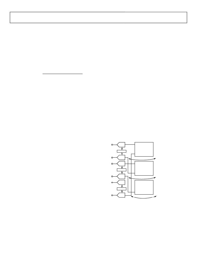
�CHANGING� PHASE� VOLTAGE� DATA� PATH�
�The� ADE7880� can� direct� one� phase� voltage� input� to� the�
�computational� data� path� of� another� phase.� For� example,� Phase� A�
�voltage� can� be� introduced� in� the� Phase� B� computational� data� path,�
�which� means� all� powers� computed� by� the� ADE7880� in� Phase� B�
�are� based� on� Phase� A� voltage� and� Phase� B� current.�
�Bits[9:8]� (VTOIA[1:0])� of� the� CONFIG� register� manage� the�
�Phase� A� voltage� measured� at� the� VAP� pin.� If� VTOIA[1:0]� =� 00�
�(default� value),� the� voltage� is� directed� to� the� Phase� A� computa-�
�tional� data� path.� If� VTOIA[1:0]� =� 01,� the� voltage� is� directed� to�
�the� Phase� B� path.� If� VTOIA[1:0]� =� 10,� the� voltage� is� directed� to� the�
�Phase� C� path.� If� VTOIA[1:0]� =� 11,� the� ADE7880� behaves� as� if�
�VTOIA[1:0]� =� 00.�
�Bits[11:10]� (VTOIB[1:0])� of� the� CONFIG� register� manage� the�
�Phase� B� voltage� measured� at� the� VBP� pin.� If� VTOIB[1:0]� =� 00�
�(default� value),� the� voltage� is� directed� to� the� Phase� B� computa-�
�tional� data� path.� If� VTOIB[1:0]� =� 01,� the� voltage� is� directed� to�
�the� Phase� C� path.� If� VTOIB[1:0]� =� 10,� the� voltage� is� directed� to�
�the� Phase� A� path.� If� VTOIB[1:0]� =� 11,� the� ADE7880� behaves�
�as� if� VTOIB[1:0]� =� 00.�
�Bits[13:12]� (VTOIC[1:0])� of� the� CONFIG� register� manage� the�
�Phase� C� voltage� measured� at� the� VCP� pin.� If� VTOIC[1:0]� =� 00�
�(default� value),� the� voltage� is� directed� to� Phase� C� computational�
�data� path,� if� VTOIC[1:0]� =� 01,� the� voltage� is� directed� to� the�
�Phase� A� path.� If� VTOIC[1:0]� =� 10,� the� voltage� is� directed� to� the�
�Phase� B� path.� If� VTOIC[1:0]� =� 11,� the� ADE7880� behaves� as� if�
�VTOIC[1:0]� =� 00.�
�IA�
�phase� voltages,� similar� to� the� ones� in� the� current� channels.� Bit� 0�
�(HPFEN)� of� CONFIG3� register� can� enable� or� disable� the� filters.�
�See� the� Current� Channel� HPF� section� for� more� details.�
�Voltage� Channel� Sampling�
�The� waveform� samples� of� the� voltage� channel� are� taken� at� the�
�output� of� HPF� and� stored� into� VAWV,� VBWV,� and� VCWV� 24-�
�bit� signed� registers� at� a� rate� of� 8� kSPS.� All� power� and� rms�
�calculations� remain� uninterrupted� during� this� process.� Bit� 17�
�(DREADY)� in� the� STATUS0� register� is� set� when� the� VAWV,�
�VBWV,� and� VCWV� registers� are� available� to� be� read� using� the�
�I� 2� C� or� SPI� serial� port.� Setting� Bit� 17� (DREADY)� in� the� MASK0�
�register� enables� an� interrupt� to� be� set� when� the� DREADY� flag� is�
�set.� See� the� Digital� Signal� Processor� section� for� more� details� on�
�VA�
�IB�
�VB�
�IC�
�VC�
�APHCAL�
�BPHCAL�
�CPHCAL�
�PHASE� A�
�COMPUTATIONAL�
�DATAPATH�
�PHASE� B�
�COMPUTATIONAL�
�DATAPATH�
�PHASE� C�
�COMPUTATIONAL�
�DATAPATH�
�VTOIA[1:0]� =� 01,�
�PHASE� A� VOLTAGE�
�DIRECTED�
�TO� PHASE� B�
�VTOIB[1:0]� =� 01,�
�PHASE� B� VOLTAGE�
�DIRECTED�
�TO� PHASE� C�
�VTOIC[1:0]� =� 01,�
�PHASE� C� VOLTAGE�
�DIRECTED�
�TO� PHASE� A�
�Bit� DREADY.�
�As� stated� in� the� Current� Waveform� Gain� Registers� section,� the�
�serial� ports� of� the� ADE7880� work� on� 32-,� 16-,� or� 8-bit� words.�
�Similar� to� registers� presented� in� Figure� 44,� the� VAWV,� VBWV,�
�Figure� 49.� Phase� Voltages� Used� in� Different� Datapaths�
��in� the� Phase� B� data� path,� the� Phase� B� voltage� is� used� in� the� Phase� C�
�data� path,� and� the� Phase� C� voltage� is� used� in� the� Phase� A� data� path.�
�and� VCWV� 24-bit� signed� registers� are� transmitted� sign�
�extended� to� 32� bits.�
�The� ADE7880� contains� an� HSDC� port� especially� designed� to�
�provide� fast� access� to� the� waveform� sample� registers.� See� the�
��Rev.� A� |� Page� 30� of� 104�
�发布紧急采购,3分钟左右您将得到回复。
相关PDF资料
EVAL-ADE7953EBZ
BOARD EVAL FOR ADE7953
EVAL-ADF4002EBZ1
BOARD EVAL FOR ADF4002
EVAL-ADG788EBZ
BOARD EVALUATION FOR ADG788
EVAL-ADM1021AEB
BOARD EVAL FOR ADM1021
EVAL-ADM1023EB
BOARD EVAL FOR ADM1023
EVAL-ADM1031EB
BOARD EVAL FOR ADM1031
EVAL-ADM1062TQEBZ
BOARD EVALUATION FOR ADM1062TQ
EVAL-ADM1075CEBZ
BOARD EVAL FOR ADM1075
相关代理商/技术参数
EVAL-ADE7880EBZ
制造商:Analog Devices 功能描述:ADE7880, ENERGY METER, 3 PH, SPI, I2C, E
EVAL-ADE7913EBZ
制造商:AD 制造商全称:Analog Devices 功能描述:3-Channel, Isolated, Sigma-Delta ADC with SPI
EVAL-ADE7953EBZ
功能描述:BOARD EVAL FOR ADE7953 RoHS:是 类别:编程器,开发系统 >> 评估演示板和套件 系列:- 标准包装:1 系列:PSoC® 主要目的:电源管理,热管理 嵌入式:- 已用 IC / 零件:- 主要属性:- 次要属性:- 已供物品:板,CD,电源
EVAL-ADF4001EBZ2
制造商:Analog Devices 功能描述:Evaluation Board For Pll Frequency Synthesizer 制造商:Analog Devices 功能描述:ADF4001 PLL SYNTHESIZER EVAL BOARD
EVAL-ADF4002EB1
制造商:Analog Devices 功能描述:EVAL BOARD - Bulk
EVAL-ADF4002EBZ1
功能描述:BOARD EVAL FOR ADF4002 RoHS:是 类别:编程器,开发系统 >> 评估演示板和套件 系列:- 产品培训模块:Obsolescence Mitigation Program 标准包装:1 系列:- 主要目的:电源管理,电池充电器 嵌入式:否 已用 IC / 零件:MAX8903A 主要属性:1 芯锂离子电池 次要属性:状态 LED 已供物品:板
EVAL-ADF4007EBZ1
功能描述:BOARD EVALUATION FOR ADF4007EB1 RoHS:是 类别:编程器,开发系统 >> 评估演示板和套件 系列:- 标准包装:1 系列:PSoC® 主要目的:电源管理,热管理 嵌入式:- 已用 IC / 零件:- 主要属性:- 次要属性:- 已供物品:板,CD,电源
EVAL-ADF4106EB1
制造商:Analog Devices 功能描述:PLL, Frequency Synthesizer